Optical Critical Dimension (OCD) and Advanced Film Analysis Metrology
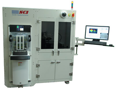
The FilmTekTM CD optical critical dimension system is SCI’s leading-edge solution for fully-automated, high-throughput CD measurement and advanced film analysis for the 1x nm design node and beyond. This system delivers real-time multi-layer stack characterization and CD measurement simultaneously, for both known and completely unknown structures.
FilmTekTM CD utilizes patented multimodal measurement technology to meet the challenging demands associated with the most complex semiconductor design features in development and production. This technology enables measurement of extremely small line widths, with high accuracy measurements in the sub-10nm range.
Existing metrology tools that rely on conventional ellipsometry or reflectometry techniques are limited in their ability to accurately resolve CD measurements in real-time, requiring tedious library generation during device research and development. FilmTekTM CD overcomes this limitation by a patented multi-modal measurement technology that provides an accurate single solution even for completely unknown structures.
FilmTekTM CD includes proprietary diffraction software with fast, real-time optimization. Real-time optimization allows the user to easily measure unknown structures with minimal setup time and recipe development while avoiding the delays and complications associated with library generation.
Key Features:
- Multimodal measurement technology for real-time multi-layer stack characterization and CD measurement at 1x nm design node and beyond.
- Multi-angle scatterometry with proprietary Rigorous Coupled Wave Analysis (RCWA)
- Normal incidence spectroscopic ellipsometry
- Spectroscopic generalized ellipsometry (4×4 matrix generalization method) with rotating compensator design
- Multi-angle, DUV-NIR polarized spectroscopic reflection (Rs, Rp, Rsp, and Rps)
- Full CD parameter measurement including period, linewidth, trench depth, and sidewall angle
- Measures film thickness and index of refraction independently
- Patented parabolic mirror technology – small spot size measures within a 50×50 µm feature
- Fast, real-time optimization allows for a wide range of applications with minimal setup time (no library generation necessary)
- Pattern recognition (Cognex)
- Cassette to cassette wafer handling
- FOUP or SMIF compatible
- SECS/GEM
Applications
- Thickness, refractive index, and optical CD metrology
- Optical constant characterization of unknown films
- Thickness of ultra-thin film stacks
- Broad range of critical dimension measurement applications including metal gate recess, high k recess, side wall angle, resist height, hard mask height, trench and contact profiles, and pitch walking
| Technical Specifications | |
|---|---|
| Film thickness range: | 0Å to 150µm |
| Film thickness accuracy: | ±1.0Å for NIST traceable standard oxide 100Å to 1µm |
| Spectral range: | 190nm to 1000nm (220nm to 1000nm is standard) |
| Measurement spot size: | 50 µm |
| Spectral resolution: | 0.3nm |
| Light source: | Regulated deuterium-halogen lamp (2,000 hrs lifetime) |
| Detector type: | 2048 pixel Sony linear CCD array |
| Computer: | Multi-core processor with Windows™ 10 Operating System |
| Measurement time: | ~2 sec (e.g., oxide film) |
| Performance Specifications | |||
|---|---|---|---|
| Film(s) | Thickness | Measured Parameters | Precision (1σ) |
| Oxide / Si | 0-1000 Å | t | 0.03 Å |
| 1000-500,000 Å | t | 0.005% | |
| 1000 Å | t , n | 0.2 Å / 0.0001 | |
| 15,000 Å | t , n | 0.5 Å / 0.0001 | |
| 150,000 Å | t , n | 1.5 Å / 0.00001 | |
| Photoresist / Si | 200-10,000 Å | t | 0.02% |
| 500-10,000 Å | t , n | 0.05% / 0.0002 | |
| Nitride / Si | 200-10,000 Å | t | 0.02% |
| 500-10,000 Å | t , n | 0.05% / 0.0005 | |
| Polysilicon / Oxide / Si | 200-10,000 Å | t Poly , t Oxide | 0.2 Å / 0.1 Å |
| 500-10,000 Å | t Poly , t Oxide | 0.2 Å / 0.0005 | |
Optional features
- To suit a wide range of budgets and end-use applications, this system is also available as a manual load, bench-top unit for R&D.