Micro-spot DUV Spectroscopic Reflectometry
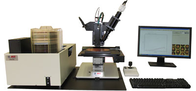
The FilmTek™ 2000 PAR is a low-cost solution for high-throughput, fully-automated mapping of patterned wafers for development and production environments. This system combines patented DUV-NIR reflectometry with wafer auto-loader and pattern recognition to deliver unmatched metrology performance at this price point.
The FilmTek™ 2000 PAR utilizes SCI’s patented parabolic mirror technology to measure wavelengths from the deep ultra-violet to the near infrared with a spot size as small as 13µm.
This system comes with advanced material modeling software to make even the most rigorous of measurement tasks reliable and intuitive. FilmTek™ software includes fully user-customizable wafer mapping capabilities to rapidly generate 2D and 3D data maps of any measured parameter. In addition to user-defined patterns, standard map patterns include polar, X-Y, rθ, or linear.
FilmTek™ 2000 PAR incorporates SCI’s generalized material model with advanced global optimization algorithms for simultaneous determination of multiple film characteristics within a fraction of 1 second per site.
Key Features:
- Automated stage with autofocus
- Automated wafer handling
- Camera for imaging measurement location
- Pattern recognition
- 50 micron spot size
Measurement Capabilities:
Simultaneous determination of:
- Multiple layer thicknesses
- Indices of refraction [ n(λ) ]
- Extinction (absorption) coefficients [ k(λ) ]
- Energy band gap [ Eg ]
- Composition (e.g., %Ge in SiGex, % Ga in GaxIn1-xAs, %Al in AlxGa1-xAs, etc.)
- Surface roughness
- Constituent, void fraction
- Crystallinity/Amorphization (e.g., degree of crystallinity of Poly-Si or GeSbTe films)
- Film gradient
Optional Features:
- Small spot size (13 µm)
- Pattern recognition (Cognex)
- Cassette to cassette wafer handling
- SECS/GEM
Applications
Virtually all translucent films ranging in thickness from less than 100 angstroms to approximately 150 microns can be measured with high precision. Typical applications include:
- Semiconductor and Dielectric materials
- Multilayer optical coatings
- Optical antireflection coatings
- Electro-optical materials
- Solar cells
- Computer disks
- Coated glass
- Laser mirrors
- Thin metals
- Biomedical
Example Films
- SiOx
- SiNx
- DLC
- SOG
- Photoresist
- Thin metals
- a-Si
- a-C:H
- ITO
- Polysilicon
- Polyimide
- Low k dielectric films
Example Substrates
- Silicon
- SOI
- SOS
- GaAs
- PET
- Aluminum
- Copper
- Glass
| Technical Specifications | |
|---|---|
| Film thickness range: | 3nm to 150µm |
| Film thickness accuracy: | ±1.5Å for NIST traceable standard oxide 1000Å to 1µm |
| Spectral range: | 190nm to 1700nm (240nm to 1000nm is standard) |
| Measurement spot size: | 13µm to 300µm (50µm is standard) |
| Wafer size: | 50mm to 300mm (150mm standard) |
| Spectral resolution: | 0.3-2nm |
| Light source: | Regulated deuterium-halogen lamp (2,000 hrs lifetime) |
| Detector type: | 2048 pixel Sony linear CCD array / 512 pixel cooled Hamamatsu InGaAs CCD array (NIR) |
| Computer: | Multi-core processor with Windows™ 10 Operating System |
| Measurement time: | <1 sec per site (e.g., oxide film) |
| Data acquisition time: | 0.2 sec |
| Performance Specifications | |||
|---|---|---|---|
| Film(s) | Thickness | Measured Parameters | Precision (1σ) |
| Oxide / Si | 200-500 Å | t | 0.5 Å |
| 500-10,000 Å | t | 0.25 Å | |
| 1000 Å | t , n | 0.25 Å / 0.001 | |
| Nitride / Si | 200-10,000 Å | t | 0.25 Å |
| Photoresist / Si | 200-10,000 Å | t | 0.5 Å |
| a-Si / Oxide / Si | 200-10,000 Å | t | 0.5 Å |