DUV-NIR Spectroscopic Reflectometry
The FilmTek™ 2000 metrology system is designed for rapid, reliable, and accurate characterization of nearly any unpatterned thin film.
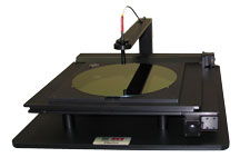
FilmTek™ 2000 is a fully-integrated package, combining a DUV-NIR fiber-optic spectrophotometer, automated stage, and advanced material modeling software to make even the most rigorous of measurement tasks reliable and intuitive.
FilmTek™ software includes fully user-customizable wafer mapping capabilities to rapidly generate 2D and 3D data maps of any measured parameter. In addition to user-defined patterns, standard map patterns include polar, X-Y, rθ or linear.
FilmTek™ 2000 incorporates SCI’s generalized material model with advanced global optimization algorithms for simultaneous determination of multiple film characteristics within a fraction of 1 second per site.
Measurement Capabilities:
Simultaneous determination of:
- Multiple layer thicknesses
- Indices of refraction [ n(λ) ]
- Extinction (absorption) coefficients [ k(λ) ]
- Energy band gap [ Eg ]
- Composition (e.g., %Ge in SiGex, % Ga in GaxIn1-xAs, %Al in AlxGa1-xAs, etc.)
- Surface roughness
- Constituent, void fraction
- Crystallinity/Amorphization (e.g., degree of crystallinity of Poly-Si or GeSbTe films)
- Film gradient
Low Cost
The cost of ownership of FilmTek™ 2000 is a small fraction of comparable automated benchtop metrology systems.
Intuitive, Completely Automated System
Fully integrated system with DUV-NIR fiber-optic spectrophotometer, automated stage, computer, and advanced material modeling software. FilmTek™ 2000 software automates measurement calibration, data acquisition and analysis so that minimal experience in thin film optical design or measurement techniques is required.
Applications
Virtually all translucent films ranging in thickness from less than 100 angstroms to approximately 150 microns can be measured with high precision. Typical applications include:
- Semiconductor and Dielectric materials
- Multilayer optical coatings
- Optical antireflection coatings
- Electro-optical materials
- Solar cells
- Computer disks
- Coated glass
- Laser mirrors
- Thin metals
- Biomedical
Example Films
- SiOx
- SiNx
- DLC
- SOG
- Photoresist
- Thin metals
- a-Si
- a-C:H
- ITO
- Polysilicon
- Polyimide
- Low k dielectric films
Example Substrates
- Silicon
- SOI
- SOS
- GaAs
- PET
- Aluminum
- Copper
- Glass
| Technical Specifications | |
|---|---|
| Film thickness range: | 5nm to 150µm |
| Film thickness accuracy: | ±1.5Å for NIST traceable standard oxide 1000Å to 1µm |
| Spectral range: | 190nm to 1700nm (240nm to 1000nm is standard) |
| Measurement spot size: | 2mm to 5mm (5mm standard) |
| Sample size: | 2mm to 300mm (150mm is standard) |
| Spectral resolution: | 0.3-2nm |
| Light source: | Regulated deuterium-halogen lamp (2,000 hrs lifetime) |
| Detector type: | 2048 pixel Sony linear CCD array / 512 pixel cooled Hamamatsu InGaAs CCD array (NIR) |
| Computer: | Multi-core processor with Windows™ 10 Operating System |
| Measurement time: | <1 sec per site (e.g., oxide film) |
| Data acquisition time: | 0.2 sec |
| Performance Specifications | |||
|---|---|---|---|
| Film(s) | Thickness | Measured Parameters | Precision (1σ) |
| Oxide / Si | 200-500 Å | t | 0.5 Å |
| 500-10,000 Å | t | 0.25 Å | |
| 1000 Å | t , n | 0.25 Å / 0.001 | |
| Nitride / Si | 200-10,000 Å | t | 0.25 Å |
| Photoresist / Si | 200-10,000 Å | t | 0.5 Å |
| a-Si / Oxide / Si | 200-10,000 Å | t | 0.5 Å |