Automated Wafer Geometry Characterization
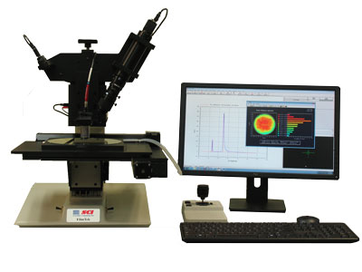
The WaferScanTM automated metrology system delivers rapid and accurate wafer geometry characterization to enable wafer manufacturers to meet the demanding lithography and CMP requirements imposed by 1x nm design rules and beyond.
Incoming wafer flatness variation, and subsequent process induced-shape changes can result in drastic reduction in final device performance and yield. WaferScanTM obtains high-throughput measurements of stress-induced wafer shape changes, shape-induced overlay, wafer thickness variation, and front-side and back-side topography to address these issues. Measurements can be performed on various substrates, including polished, epitaxial and SOI wafers.
Key Features:
- Chromatic confocal spectroscopy
Measurement Capabilities:
- Wafer bow and warp
- Stress-induced curvature
- Wafer thickness and flatness variation
- Front and back surface topography
- Wafer edge roll-off (ERO)
Optional Features:
- Cassette to cassette wafer handling
- FOUP and SMIF compatible
- SECS/GEM
| Technical Specifications | |
|---|---|
| Wafer thickness range: | 5 μm – 1.5 mm |
| Wafer thickness accuracy: | ± 1.0 μm |
| Wafer thickness precision: | 0.1 μm |
| Thickness resolution: | 0.01 μm |
| Wafer curvature range: | Up to 1.5 mm |
| Spectral range: | 400 nm – 1000 nm |
| Measurement spot size: | 25 µm |
| Spectral resolution: | 0.3 nm |
| Light source: | Regulated halogen lamp (10,000 hrs lifetime) |
| Detector type: | 2048 pixel Sony linear CCD array |
| Automated Stage with Auto Focus | 300mm (200mm is standard) |
| Computer: | Multi-core processor with Windows™ 10 Operating System |