Through Silicon Via (TSV) Metrology
FilmTek™ 2000M TSV Metrology Advantages
- Fully automated metrology platform for fast and reliable critical dimension, etch depth, and film thickness measurement over a wide range of TSV sizes and aspect ratios
- CD precision (1σ) < 0.2%
- Etch depth precision (1σ) < 0.005%
- Film thickness range: 10nm – 350μm
- Film thickness precision (1σ) < 0.005%
- Measurement time of 1-2 seconds per point
- Pattern recognition by Cognex
- Lowest total cost of ownership
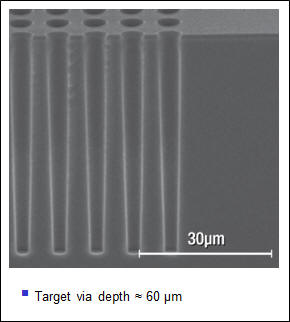
Depth Measurement of High Aspect Ratio TSV Structures
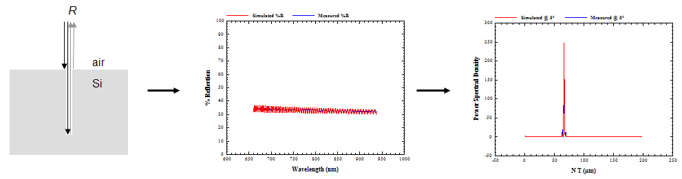
- Interference between reflected waves is caused by optical path length difference between the top and bottom surfaces of the TSV structure
- The spot size must be small (same order as via diameter) and the measurement beam must be nearly collimated to observe interference in the reflected light
- Patented FilmTek™ technology allows a small measurement spot size without the use of a high power objective
Case Study: Comparison of TSV Etch Depth by FilmTek™ 2000M TSV and SEM
| Via Diameter (µm) | Etch Depth (µm) SEM | Etch Depth (μm) FilmTek™ 2000M TSV |
|---|---|---|
| 5 | 44.5 | 44.3 |
| 10 | 55.5 | 55.5 |
| 15 | 62.0 | 61.8 |
| 20 | 66.5 | 66.8 |
- Excellent agreement between FilmTek™ 2000M TSV and SEM data