Photovoltaics: Characterizing Thin Film Solar Cells
FilmTek™ 2000 Advantages
- Reflection spectrophotometry allows for fast and accurate characterization of thin film solar cells.
- Simultaneous measurement of layer thicknesses, interfacial layers, and surface roughness.
- Uses a general dispersion model to describe the optical response. This reduces the number of fitted parameters required and eliminates multiple solutions.
- Measurement and analysis time of ~1 second per point.
Thin Film Solar Cells
Thin film solar cell technologies have substantial cost advantages over traditional silicon photovoltaic cells because of the reduced amount of semiconductor material necessary for the construction of the device. Typical thin film solar cells use only a few microns of active material on glass compared to hundreds of microns used for a wafer based cell. In general, thin film solar cells use a thin layer of photo-electrically active material deposited between thin conductive films serving as electrodes on a glass substrate. One electrode will be a transparent conducting oxide (TCO) and is commonly made from indium tin oxide or aluminum doped zinc oxide, while the second electrode usually consists of metals. There are various intrinsic and compound semiconductor materials which are suitable for the light absorbing layer, but the primary commercial technologies for thin film devices are based on amorphous silicon (a-Si), cadmium telluride (CdTe) and copper indium gallium di-selenide (CIGS).
For solar cells, multiple levels of amorphous and/or micro-crystalline silicon must be carefully deposited over very large areas. The various layers as well as the interfaces between the layers have to be precisely controlled to achieve the maximum light-to-electricity conversion (solar cell efficiency).
Our FilmTek™ thin film metrology tools are being increasingly used in solar cell applications to characterize the various layers and interfaces during solar cell production. The information generated from FilmTek™ measurements allows for greater process control, which results in higher yield and device efficiencies. Greater process control is a key factor required for reducing the future costs of photovoltaic cells. FilmTek™ thin film metrology tools can be used for photovoltaic device characterization for all of the primary thin film solar cell technologies. Our current installed customer base includes the largest manufacturer of CdTe based solar cells and several a-Si based solar cell companies.
Amorphous Silicon (a-Si)
Amorphous solids, like common glass, are materials in which the atoms are not arranged in any particular order. They do not form crystalline structures at all, and they contain large numbers of structural and bonding defects. Amorphous silicon applies to photovoltaic technology if the deposition conditions are properly controlled and if composition is carefully modified.
Amorphous silicon absorbs solar radiation 40 times more efficiently than single-crystal silicon, so a film only 1 micron thick can absorb 90 percent of the usable solar energy. Today, amorphous silicon is the most common form of thin film photovoltaic and is ideal for low-powered consumer devices.
Unlike a crystal, the atoms of amorphous materials are randomly disordered from the crystalline positions. Amorphous silicon is used in photovoltaic devices by controlling its deposition conditions and by carefully modifying its doping. With optical engineering, the thin film, often only 1 micron thick, can absorb a high percentage of the usable solar energy. Amorphous silicon is currently the predominant thin film photovoltaic type. It is most often used for low-power consumer devices (like wristwatches and calculators) and other power applications that are not space constrained. The a-Si manufacturing process is perhaps the simplest of the thin film photovoltaic types.
Cadmium Telluride (CdTe)
Cadmium telluride, another thin film technology, has cell efficiencies of over 16% in the laboratory. However, CdTe exhibits certain limitations that keep the technology from full market acceptance, including cadmium’s heavy metal characteristics and tendency to degrade electronic contacts outdoors. Also, CdTe deposition and crystal formation requires high processing temperatures. CdTe is only manufactured in a configuration in which sunlight must pass through the substrate to get to the photovoltaic material. Glass is the only material that can withstand the temperature and still be adequately transparent. Due to its fragile nature, the glass must be thick and heavy to endure the stresses found during product life in the field.
Copper Indium Gallium di-Selenide (CIGS)
Copper indium di-selenide (CuInSe2) has an extremely high absorption that allows 99 percent of available light to be absorbed in the first micron of the material. This makes it an optimal, effective photovoltaic material. Adding small amounts of gallium to the CuInSe2 boosts its light-absorbing band gap, which makes it more closely match the solar spectrum, thereby improving the voltage and the efficiency of the photovoltaic cell. CIGS cells have reached conversion efficiencies of more than 19 percent – much higher than other thin film photovoltaics. This high conversion efficiency remains stable over time for reliable performance. CIGS also passes environmental certification and waste-handling requirements.
Using FilmTekTM Tools to Increase Solar Cell Efficiency
Solar cell efficiency is one measure of the performance of a photovoltaic product, defining what percentage of the energy in sunlight is actually converted into electricity by the photovoltaic device. It has been observed that a 1-percentage point increase in efficiency typically reduces solar cell production costs by 5 to 8 percent.
Methods for increasing the maximum achievable current density of amorphous silicon solar cells include bandgap and layer thickness optimization. Additionally, light confinement strategies such as textured interfaces are used to enhance the absorption in the active semiconductor layer. Scattering at rough interfaces inside the solar cell leads to enhanced absorption due to an increased optical path length in the layers. However, the rough interfaces can lead to both enhancement and deterioration of the optical performance of the a-Si solar cell. Accurate characterization of the band gap, layer thicknesses, and rough interfacial layers is critical for maximizing photovoltaic device efficiency.
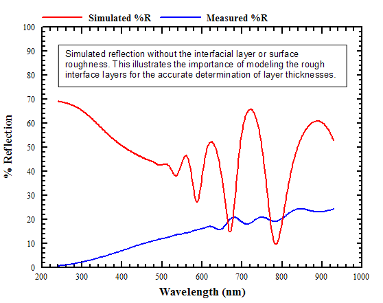
The FilmTek™ 2000 thin film metrology tool readily measures these photovoltaic device parameters using non-contact reflection spectrophotometry. In addition to the physical oscillator models used to describe the TCO and a-Si materials, FilmTek™ 2000 uses a proprietary interfacial roughness model to describe the interfacial layer between the TCO and a-Si layers. Proper modeling of this rough interfacial layer is critical for accurate determination of the solar cell layer thicknesses, band gap, and surface roughness.
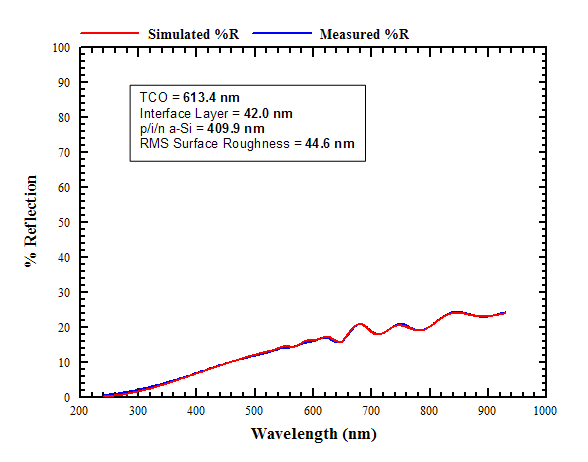
For example, consider the following solar cell with TCO and p/i/n amorphous silicon layers. The FilmTek™ 2000 accurately and simultaneously determines the solar cell layer thicknesses and surface roughness in about 1 second.
However, consider the same device measurement without modeling the effects of the interfacial layer or surface roughness. The simulated reflection is very different than the measured reflection, making the accurate determination of the layer thicknesses impossible.