Micro-spot size Reflection and Transmission Spectrophotometry
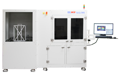
The FilmTek™ 3000M combined reflection-transmission metrology system was developed for efficient and accurate measurement of patterned films deposited on transparent substrates. The FilmTek™ 3000M utilizes allows for a small spot size down to 2 µm, and can be equipped with a large custom stage for flat panel display applications.
Conventional optical metrology systems which utilize a high power objective for sub-15µm spot measurements are prone to significant signal degradation and optical artifacts, limiting their use for patterned samples, non-uniform films, and thick films. The patented optical design of FilmTek™ 3000M maintains high signal fidelity even during small spot measurements by allowing for a sub-10µm spot with a low power objective. Avoiding the use of a high power objective is critical for limiting the angular spectrum of the collected light and maximizing the coherence of both spectral reflection and transmission.
FilmTek™ 3000M capabilities can be expanded to perform fully-automated imaging-based critical dimension (CD) measurement of patterned samples. This option allows for simultaneous CD and film thickness measurement.
FilmTek™ 3000M is a fully-integrated package, with advanced material modeling software to make even the most rigorous of measurement tasks reliable and intuitive.
Key Features:
- Spectroscopic reflection
- Spectroscopic transmission
- 5nm to 350µm film thickness range
- 2µm spot size (5×10µm standard)
- Automated stage with autofocus
- Camera for imaging measurement location
- Pattern recognition
Measurement Capabilities:
FilmTek™ 3000M incorporates SCI’s generalized material model with advanced global optimization algorithms for simultaneous determination of:
- Multiple layer thicknesses
- Indices of refraction [ n(λ) ]
- Extinction (absorption) coefficients [ k(λ) ]
- Energy band gap [ Eg ]
- Critical dimension (CD) measurement
Optional Features:
- Automated flat panel/wafer handling
- Flat panel total thickness variation (TTV) measurement
- SECS/GEM
| Technical Specifications | |
|---|---|
| Film thickness range: | 5nm to 350µm (5nm to 150µm is standard) |
| Film thickness accuracy: | ±1.5Å for NIST traceable standard oxide 1000Å to 1µm |
| CD precision (1σ): | <0.2% |
| Spectral range: | 380nm to 1700nm ( 380nm to 1000nm is standard) |
| Measurement spot size: | 2µm (5×10µm standard with 10x objective) |
| Sample size: | 2mm to 600mm (150mm is standard) |
| Spectral resolution: | 0.3-2nm |
| Light source: | Regulated halogen lamp (2,000 hrs lifetime) |
| Detector type: | 2048 pixel Sony linear CCD array / 512 pixel cooled Hamamatsu InGaAs CCD array (NIR) |
| Computer: | Multi-core processor with Windows™ 10 Operating System |
| Measurement time: | <1 sec per site (e.g., oxide film) |
| Performance Specifications | |||
|---|---|---|---|
| Film(s) | Thickness | Measured Parameters | Precision (1σ) |
| Oxide / Si | 50-1000 nm | t | 0.025 nm |
| 1-150 µm |
t | 0.005% | |